
 Schematic & PCB Design

 Simulation

 Prototype/Pilot/MP Production Support
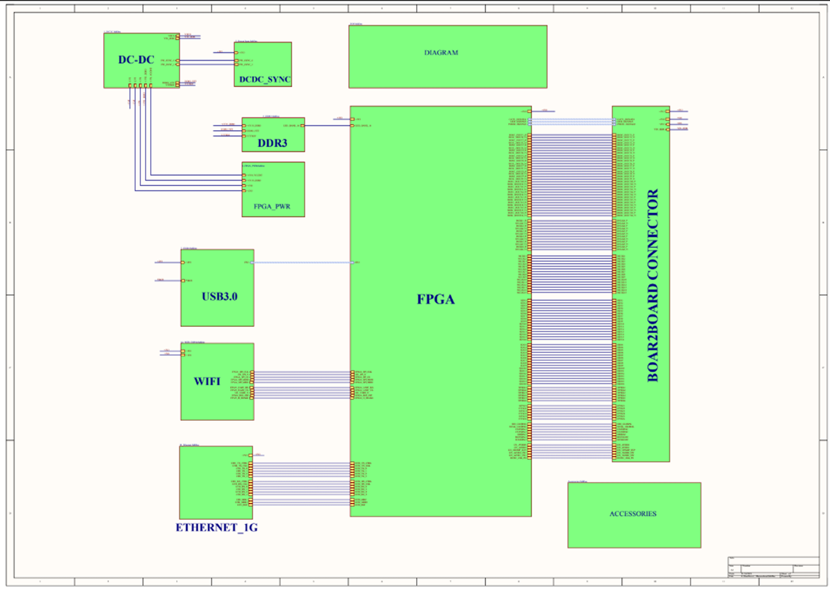
Principle design: The diagram is organized into functional blocks, hierarchical, easy to read, and suitable for complex systems.
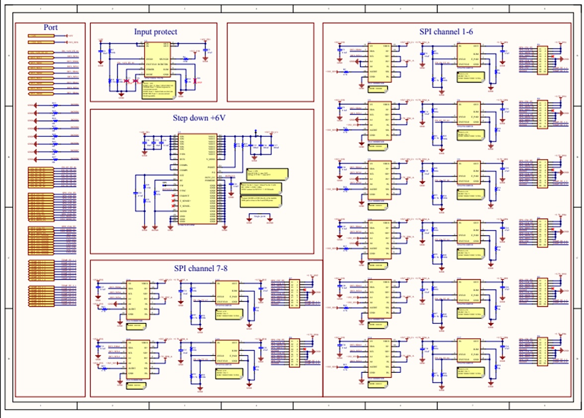
Principle design: Consistent notation, standardized signal naming, and a clear layout simplify design review and expansion.
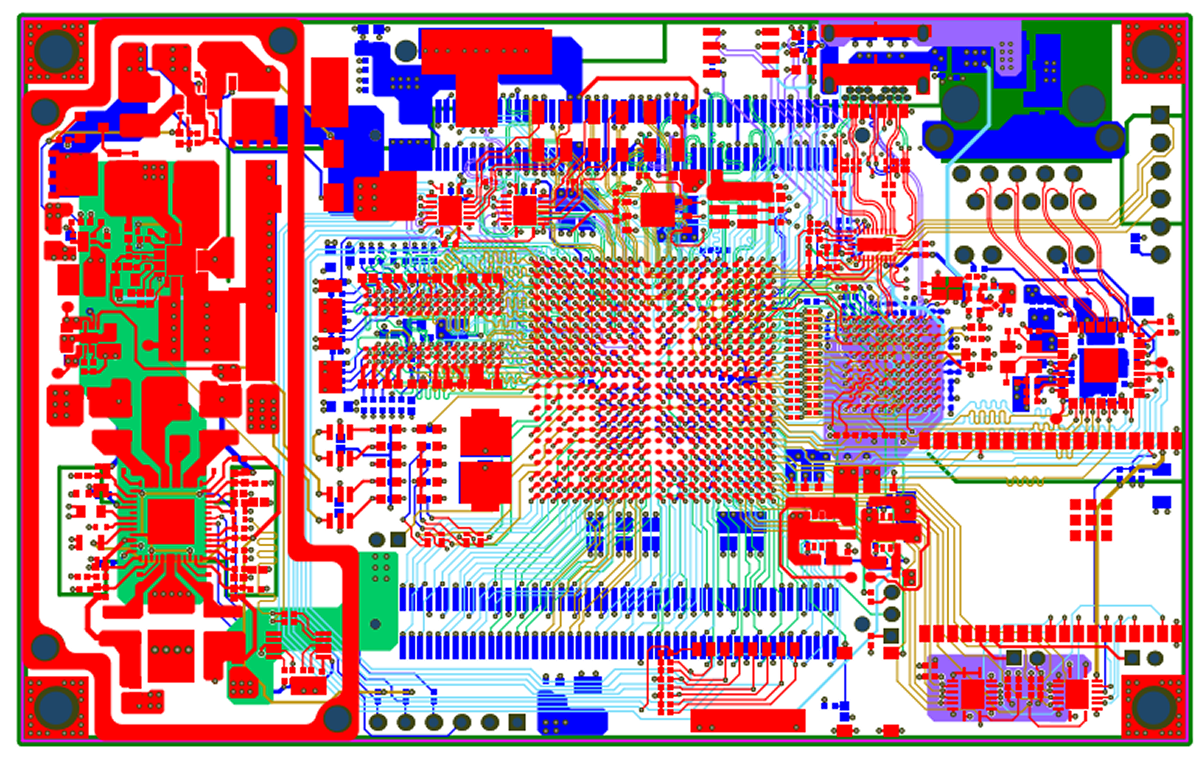
PCB design: Multi-layer stacking (16 layers) optimized for high-speed, cascaded power supply, noise control, and ensuring stable performance for demanding applications.

PCB design: DDR4 design, impedance control, SI/EMI optimization, and ensuring the return path meets standards.
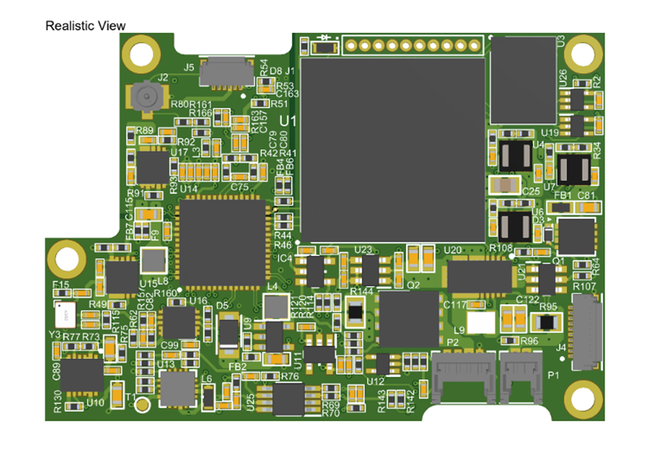
PCB design: Optimal analog-digital layout, noise reduction, optimized grounding, and design feasibility within limited space.
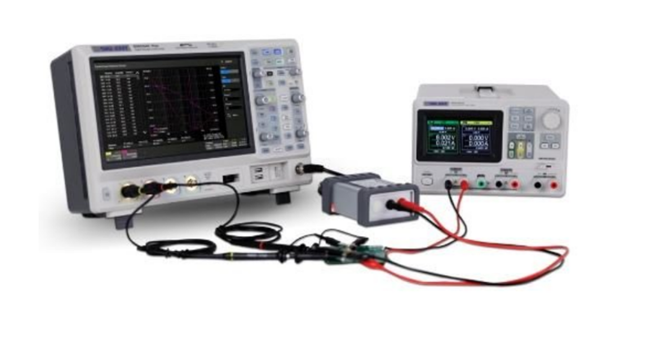
Bring-up/Debug Support: We provide bring-up and debugging support for new designs using oscilloscopes, DC power supplies, and specialized measuring equipment.
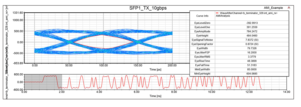
SI/PI simulations are conducted to evaluate signal quality by performing impedance sweeps and transmission-line modeling, ensuring that both signal amplitude and eye opening meet the required specifications for high-speed communication interfaces.
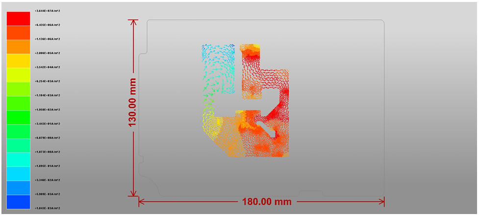
Identifies regions of high electron current density that cause localized heating, supporting layout optimization to improve reliability and reduce the risk of component failure.
l08_pwr2 (Voltage Plot)
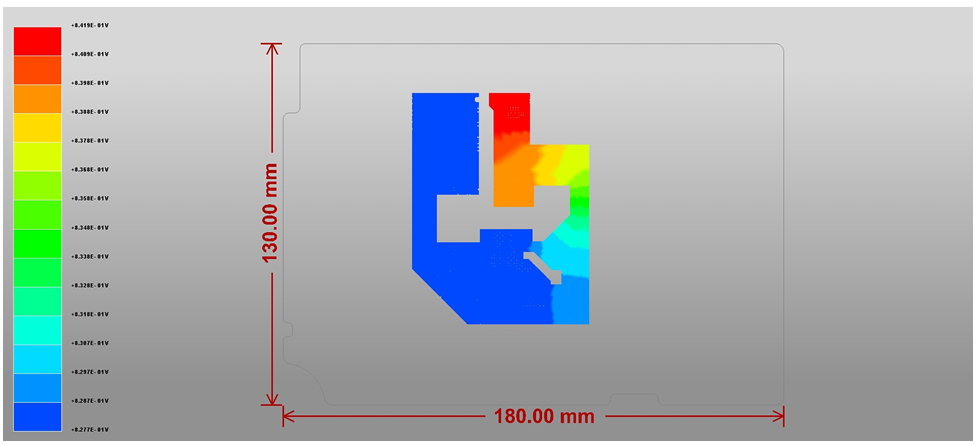
l09_pwr3 (Voltage Plot)
l10_pwr4 (Voltage Plot)
l11_gnd4 (Voltage Plot)
Simulates current distribution and voltage drop across the entire board, enabling optimization of power delivery paths, minimizing voltage loss, and improving overall system stability.


